Generating sine wave signal using PIC1xf series is a common project in internet but most of the source code is written in assembly language. Assembly language is good and efficient but it is not portable as C language.


Result:

I found a series of tutorials at tahmidmc blog.
The blog explains the sine wave pwm generation from head to toe.
Always start with tutorials for learning.
The key of sine wave is the sine wave duty cycle constants,
tahmidmc has created a useful program to generate sine wave constants.
It is a handy and easy to use but it requires installation which i do not like.
How TO Use the Software
There are two types of sinusoidal pwm, unipolar pwm and bipolar pwm.
For unipolar pwm, only need two pwm to form sinusoidal wave.
For bipolar pwm, need four pwm to form sinusoidal wave but the DC voltage needed only Vpeak, while unipolar pwm need DC voltage which is double of Vpeak.
At smart sine, for unipolar pwm, you need to add offset to get full sine wave.
A simple example, would be as follow:
Use the 32 samples for better viewing, purpose, but the sample entries can be changed to get desired sine wave frequency.
Example,
PWM frequency: 20kHz, sine wave frequency = 50Hz.
Sample = (PWM frequency) / (sine wave frequency)
= (20 000) / (50) = 400
Always tune the PWM frequency to get desired sine wave frequency as the sample entries can be changed.
Now for the PWM settings - ECCP1CON (8 bits)
P1M1:P1M0: Enhanced PWM Output Configuration bits
10 = Half-bridge output: P1A, P1B modulated with dead-band control; P1C, P1D assigned as port pins
DC1B1:DC1B0: PWM Duty Cycle Bit 1 and Bit 0
PWM mode:
These bits are the two LSbs of the 10-bit PWM duty cycle. The eight MSbs of the duty cycle are found in CCPR1L.
CCP1M3:CCP1M0: Enhanced CCP Mode Select bits
1100 = PWM mode: P1A, P1C active-high; P1B, P1D active-high
1101 = PWM mode: P1A, P1C active-high; P1B, P1D active-low
1110 = PWM mode: P1A, P1C active-low; P1B, P1D active-high
1111 = PWM mode: P1A, P1C active-low; P1B, P1D active-low
For dual mode pin assignment,

To skip the datasheet details, it is good to read block diagram,

Half bridge PWM output

The PIC18f enhanced PWM has dead band control which is good for high side and low side switch control. Power transistor has faster switch on time but slower switch off, if both high and low side is switched at the same time, a very high current (shoot-through current) may flow through both power switches, shorting the bridge supply.
Dead band delay allow switch to fully turned off before switch on another power transistor.
ECCP1DEL: PWM DEAD-BAND DELAY REGISTER
PDC6:PDC0: PWM Delay Count bits
Delay time, in number of FOSC/4 (4 * TOSC) cycles, between the scheduled and actual time for a PWM signal to transition to active.
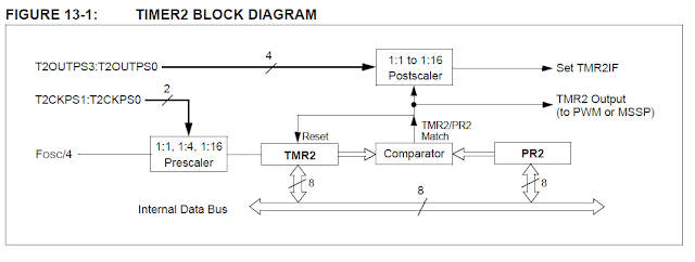
Another important module associated with PWM is timer2. Just for reference,

Now we have all the details need to write the code:
1 2 3 4 5 6 7 8 9 10 11 12 13 14 15 16 17 18 19 20 21 22 23 24 25 26 27 28 29 30 31 32 33 34 35 36 37 38 39 40 41 42 43 44 45 46 47 48 49 50 51 52 53 54 55 56 57 58 59 60 61 62 63 64 65 66 67 68 69 70 71 72 73 74 75 76 77 78 79 80 81 82 83 84 85 86 87 88 89 90 91 92 93 94 95 96 97 98 99 100 101 102 103 104 105 106 107 108 109 110 111 112 113 114 115 116 117 118 119 120 121 122 123 124 125 | #include <p18f4553.h> //****************************************************************************** // CONFIG //****************************************************************************** #pragma config PLLDIV = 5 // (20 MHz crystal on PICDEM FS USB board) #pragma config CPUDIV = OSC1_PLL2 #pragma config USBDIV = 2 // Clock source from 96MHz PLL/2 #pragma config FOSC = HSPLL_HS #pragma config FCMEN = OFF #pragma config IESO = OFF #pragma config PWRT = OFF #pragma config BOR = ON #pragma config BORV = 3 #pragma config VREGEN = ON //USB Voltage Regulator #pragma config WDT = OFF #pragma config WDTPS = 32768 #pragma config MCLRE = ON #pragma config LPT1OSC = OFF #pragma config PBADEN = OFF // #pragma config CCP2MX = ON #pragma config STVREN = ON #pragma config LVP = OFF // #pragma config ICPRT = OFF // Dedicated In-Circuit Debug/Programming #pragma config XINST = OFF // Extended Instruction Set #pragma config CP0 = OFF #pragma config CP1 = OFF // #pragma config CP2 = OFF // #pragma config CP3 = OFF #pragma config CPB = OFF // #pragma config CPD = OFF #pragma config WRT0 = OFF #pragma config WRT1 = OFF // #pragma config WRT2 = OFF // #pragma config WRT3 = OFF #pragma config WRTB = OFF // Boot Block Write Protection #pragma config WRTC = OFF // #pragma config WRTD = OFF #pragma config EBTR0 = OFF #pragma config EBTR1 = OFF // #pragma config EBTR2 = OFF // #pragma config EBTR3 = OFF #pragma config EBTRB = OFF const rom unsigned int unipolar_32_sine_wave_constant [32] = { 511, 611, 707, 795, 872, 936, 983, 1012, 1022, 1012, 983, 936, 872, 795, 707, 611, 511, 411, 315, 227, 150, 86, 39, 10, 0, 10, 39, 86, 150, 227, 315, 411 }; struct pwm_settings { unsigned char mode; unsigned int duty_cycle; unsigned int frequency; }; struct pwm_settings pwm; unsigned char counter=0; void main() { RCONbits.IPEN=1; // set the dual mode ECCP1CONbits.P1M = 0b10; ECCP1CONbits.CCP1M = 0b1101; // set the pin output TRISCbits.TRISC2 = 0; TRISDbits.TRISD5 = 0; //--------------------------------------------------- // set timer 2 T2CONbits.T2CKPS = 0b00; T2CONbits.TOUTPS = 0b0000; T2CONbits.TMR2ON = 0; // STOP TIMER2 registers to POR state PIE1bits.TMR2IE = 0; // Disable Timer2 overflow interrupts PR2 = 0xFF; // Set period //--------------------------------------------------- // set dead-bank delay ECCP1DELbits.PDC = 0b000000; CCPR1L = 0xFF; ECCP1CONbits.DC1B = 0b00; INTCONbits.GIEH=1; T2CONbits.TMR2ON = 1; // Enable TIMER2 registers to POR state PIE1bits.TMR2IE = 1; // Enable Timer2 overflow interrupts } //---------------------------------------------------------------------------- // High priority interrupt vector void InterruptHandlerHigh() ; #pragma code InterruptVectorHigh = 0x08 void InterruptVectorHigh(void) { _asm goto InterruptHandlerHigh //jump to interrupt routine _endasm } //---------------------------------------------------------------------------- // High priority interrupt routine #pragma code #pragma interrupt InterruptHandlerHigh // // Timer0 overflow void InterruptHandlerHigh() { if (PIR1bits.TMR2IF) PIR1bits.TMR2IF = 0; counter++; if(counter >= 32) counter=0; pwm.duty_cycle = unipolar_32_sine_wave_constant[counter]; /* Duty cycle PWM port1 */ CCPR1L = (unsigned char) (pwm.duty_cycle >> 2); ECCP1CONbits.DC1B = (unsigned char) (pwm.duty_cycle); } |
Result:
No comments:
Post a Comment